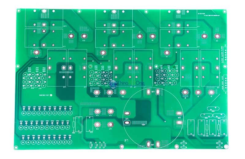
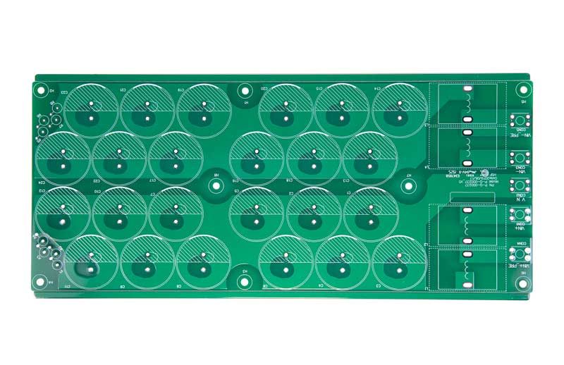
Heavy Copper PCB
1, Heavy copper definition
Generally, copper foil with a thickness of 105μm (per unit area 3oz/ft²) and above is collectively referred to as heavy copper foil, and copper foil with a thickness of 300μm and above is called ultra-heavy copper foil, made of heavy copper foil and ultra-heavy copper foil PCB is called "heavy copper printed circuit board". Compared with conventional printed circuit boards, the most prominent advantage of this type of heavy copper printed circuit board in terms of performance is that it can stably pass large currents and can better dissipate the heat generated by the load high current, so it is also called high-current printed circuit board.
2, Heavy copper printed circuit board applications
Heavy copper mainly solves the needs of high power and high current. This kind of demand is increasing in the power energy, automobile industry, computer, solar energy, military and other industries. It can replace the traditional cable wiring and metal strips. Etc. transmission structure can not only improve production efficiency, but also reduce wiring and system maintenance costs.
3, Heavy copper printed circuit board production
Compared with the production of ordinary boards, the production process of thick copper foil printed circuit boards has many difficulties. The etching accuracy, laminated structure, drilling processing, and solder mask printing all have their own special difficulties. Currently ,there are three main methods for making heavy copper:
-
A, Electroplating
Because of the scarcity of thick copper foil in the market, the thickness of the factory's standing copper foil is generally only 5OZ. Some thick copper foil orders that exceed the thickness are processed by the factory using 5OZ copper foil and then electroplating thickening. Taking into account the overall processing cost (plating time too long, the production capacity of electroplating equipment is too high) and difficulty (etching uniformity caused by electroplating uniformity). Generally, the heavy copper thickness of electroplating is limited to less than 3OZ, and the actual copper thickness is less than 8OZ.
-
B, Lamination
It is to laminate a layer of ultra-heavy copper foil directly. Although this method has better copper thickness uniformity than the electroplating thickening method, it still requires multiple etchings. The bottom etching residue of the line width is large, and the solder mask printing is difficult to process. difficulty. The wiring density is also limited.
-
c, Heavy copper foil etching & lamination
This method is made by etching the front and back sides of the copper foil. Before lamination, one side of the copper foil is used to etch a half-depth pattern, and then the etched pattern is pressed into the core board, and then processed according to the normal process after lamination. When the second side is etched, the remaining copper thickness is etched through, and the substrate part is etched, and the first pattern is pressed inside the substrate. The advantage is that the copper thickness of the two etchings is reduced, which is conducive to the control of the line width, the copper thickness exposed outside the substrate is also reduced, and the difficulty of solder mask printing is also increased. The main difficulty lies in the alignment of the two pattern etchings and the calculation of the PP filling amount for pressing. Our company's thick copper foil circuit boards above 6OZ mainly adopt this process.
4, Difficulties in the production of heavy copper PCBs
-
A, Copper foil
Generally ,heavy copper plates have higher voltage resistance requirements, so the surface roughness (Rz) of the copper foil is required to be low and uniform, because this determines whether thin core boards (under 125μm) can be used in ultra-heavy copper printed circuit boards , or Can it achieve a lower finished thickness of the printed board.
-
B, Pressing
The heavy copper foil printed circuit board is prone to problems such as insufficient filling, large flow of glue, uneven thickness, and voids during the pressing process because of the thick copper. In pressing, you should try to choose PP (1080 or 106) with a large amount of glue to press, and choose the number of PP sheets according to the actual filling requirements to ensure that the filling is sufficient and not excessive, resulting in a pressing slide.
-
C, Drilling
When the heavy copper printed circuit board in drilling process, due to the overall proportion of copper is relatively high, especially when the multi-layer heavy copper is drilled, the drill bit heats up rapidly when the drill is rotated, and the copper wire under cutting is easy to cut the drill edge. Damage, resulting in the roughness of the hole wall and the nail head being too large, causing the via failure during welding. Therefore, choosing the right drill bit and parameters is the key to processing. At the same time, the minimum aperture should be designed to be above 0.4mm as much as possible during the design. The thicker the copper, the higher the number of layers, and the larger the aperture, the more conducive to production and processing. Our company has separate drilling parameters for heavy copper foil circuit boards, which can maintain the smooth roughness of the hole wall and good hole quality.
-
D, Etching
During the etching process, the etching solution will attack the side of the line, causing side corrosion, making the actual line width smaller than the design line width. The thicker the copper, the longer the etching time will be. The side corrosion is also greater. In order to compensate for the impact of side corrosion, the PCB production draft will pre-compensate the line width, but the line width compensation will reduce the line spacing and increase the etching time, so different copper thicknesses, there are different requirements for the design line width/line spacing. The following are the design recommendations for line width/line spacing based on our process capability (unit: mil):

5, Production of our company
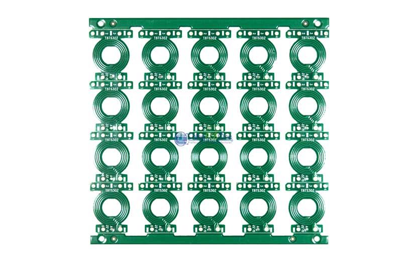
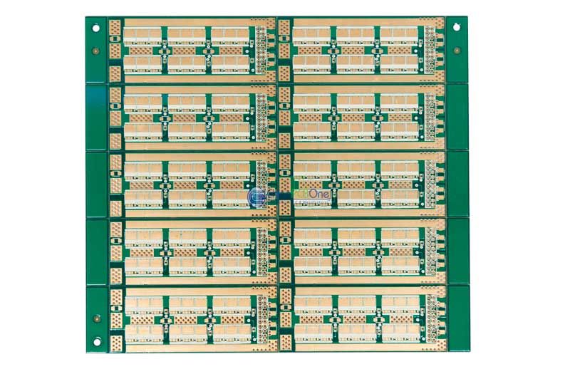
Halogen-free FR4 TG150 PCB
Layer Count: 12
Raw Material: Halogen-free FR4 TG150
Surface Treatment: OSP
Special Process: inner copper thickness 5oz, outer copper thickness 2oz,impedance control
Application: Mobile phone fast charging

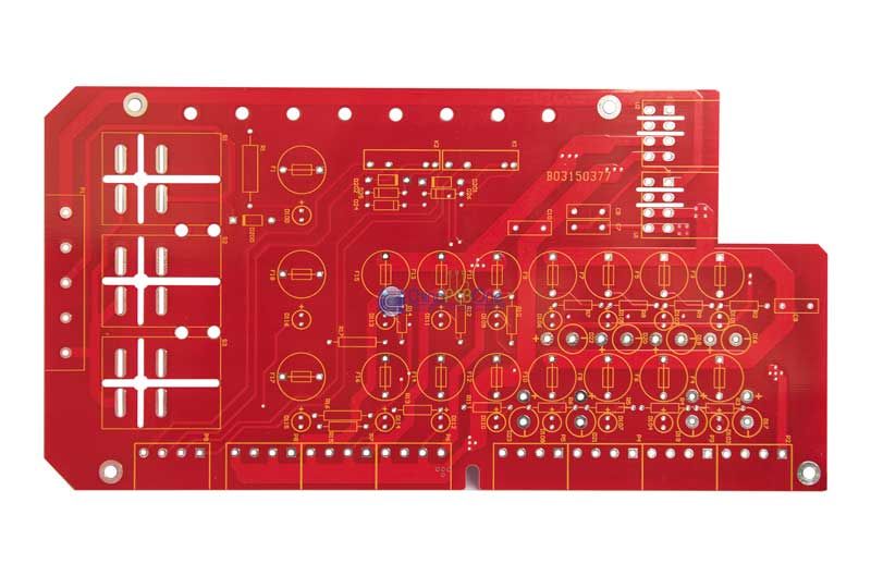
FR4 TG170 PCB
Layer Count: 2
Raw Material:FR4 TG170
Surface Treatment: Immersion Gold(ENIG)
Special Process: finished copper thickness 15oz
Application: High power supply
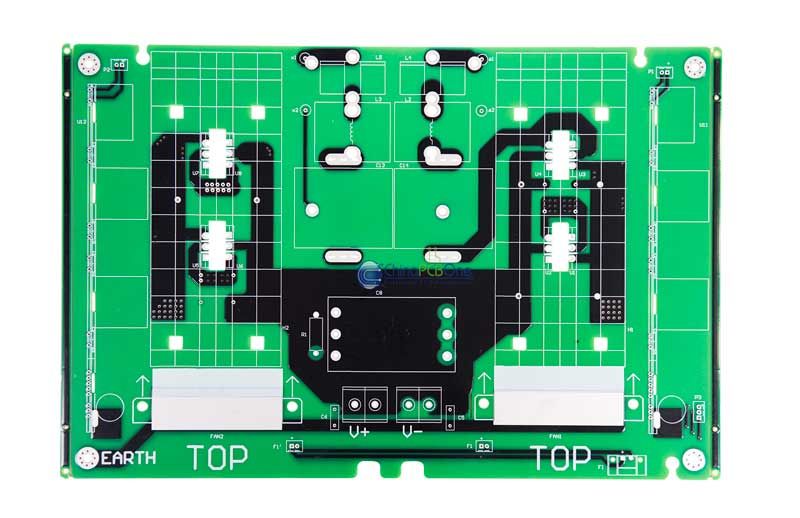
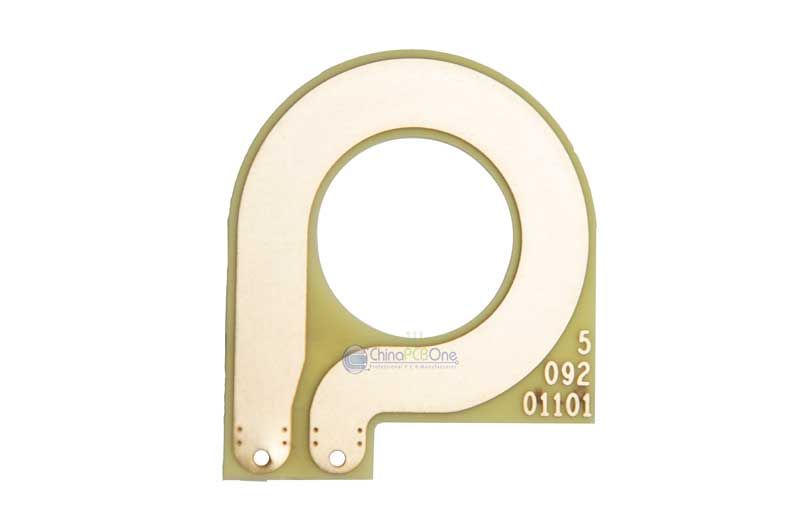
FR4 TG170 PCB
Layer Count: 2
Raw Material: FR4 TG170
Surface Treatment: Immersion Tin
Special Process: Finished copper thickness 9oz
Application: Power supply module
We have a professional R&D team with over 10 years of experience in processing heavy copper foil circuit boards. We always have 4OZ, 5OZ, 8OZ, and 10 OZ copper foils to ensure that we can respond quickly and deliver within one week as soon as possible.
ABOUT US
contact us
Tel:+86-13612807580
Fax:+86-755-23063520
Email:This email address is being protected from spambots. You need JavaScript enabled to view it.

