Multi-layer PCB
Our market is the Multilayer PCB(40L), HDI PCB(2 steps), Special process & Special material PCB, such as Aluminum base PCB, Rigid-Flex PCB, High-Frequency PCB, Heavy Copper PCB ( 19OZ ), and so on.
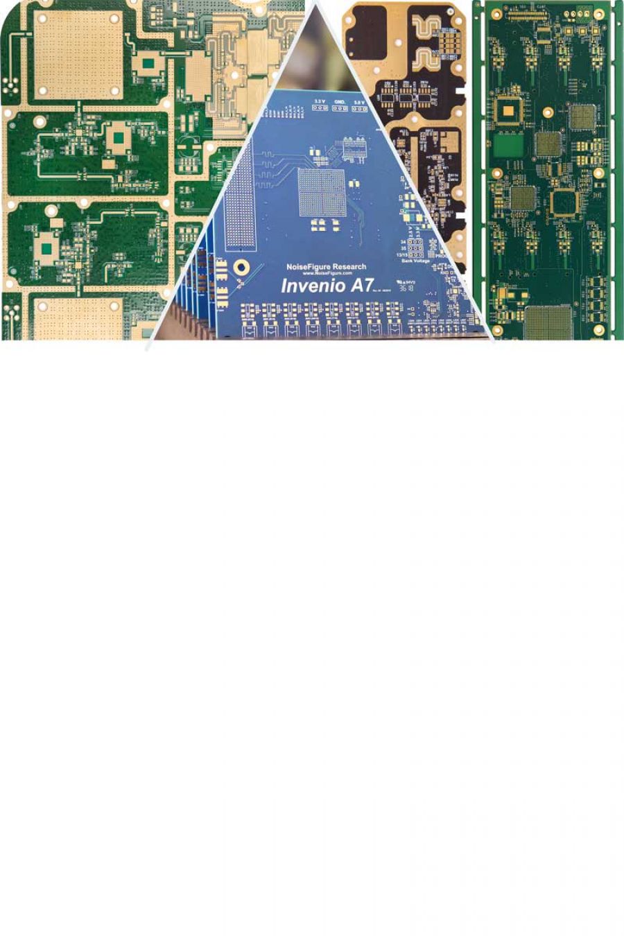
Multilayer Printed Circuit Board
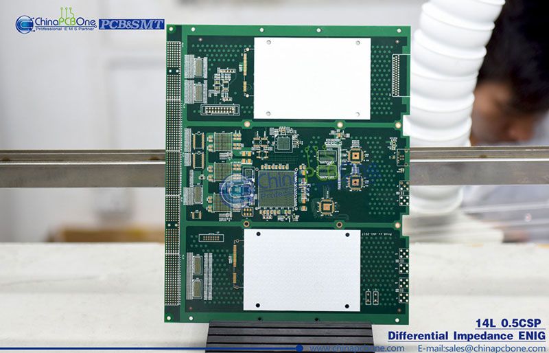
We can produce up to 40 layers of high-layer circuit boards, various buried and blind vias circuit boards, and HID PCB. HDI PCB can be up to 2 steps.
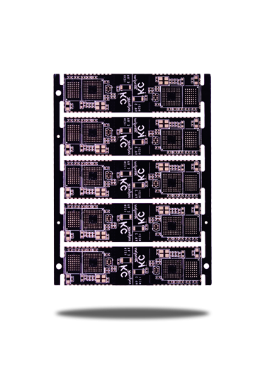
High-difficult PCB
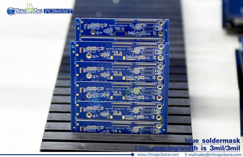
①: Min hole we can drill is 0.15mm, and 0.075mm for HDI design, and high-density print circuit board. ②: We can control impedance both single-end and differential for multi-layer(the min trace width/space is 4mil/4mil) ③: High precision circuit board( min trace width we can do 3mil, and the thinnest core we can do is 0.05mm) ④: Other special material board
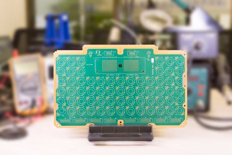
Special Material
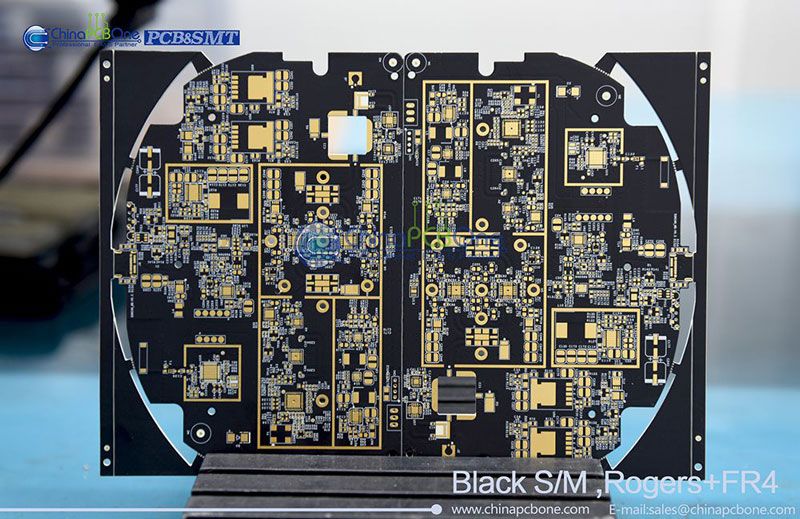
Heavy copper board( copper weight:210-700um), copper base material, aluminum, PI material, BT material, high-frequency material, Rogers Series, PTFE material, Taconic Series, Arlon.
Special Technology
①: Flex-rigid board, high to six layer flex in the inner layer, gold finger in flex area. ②: Steps boards: can expose the pad and circuit for inner circuit ③: Mixture surface treatment: OSP+ENIG ④: Multi-layer metal board: double side copper baseboard, double side aluminum board. ⑤: Mixture laminating: can process two or more material mixture laminating, like Ceramic +FR4+PTFE ⑥: Multi-frequency board: every board use high-frequency material ⑦: Plugging resin
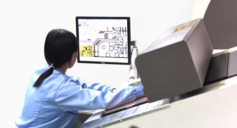
High-Quality Insurance
Processing high quality is the essential requirement for every staff
①: We strictly train and test the operation for staff
②: The quality department will check every status for all the board, to ensure the board can meet the quality requirement.
③: Providing all test equipment( like AOI, fly probe machine and all kinds of test machine), so that can ensure and improve the quality checking.
The Application for Multi-layer PCB
Including Electronic consumption, Industrial manufacturing, LED lighting, electric power, Bluetooth communication, Radar antenna, aviation, automobile, and high-frequency communication.
Special Material for PCB
Normal FR4, high TG FR4, PTFE, ceramic, aluminum, metal base, flex material, BT, PI, and so on.
Special Process for PcB
Include FR4+ceramic laminating, PTFE+FR4 laminating, heavy copper, flex-rigid, multi-layer, and impedance control. Also, we can process blind& buried hole, via in pad, plugging resin and countersink, and so on special process. Besides, we can process step boards with professional experience.
One-Stop Shop Service for
PCBA & PCB Manufacturing
Online Services

ABOUT US
contact us
Tel:+86-13612807580
Fax:+86-755-23063520
Email:This email address is being protected from spambots. You need JavaScript enabled to view it.